Imagine for a moment that you are asked to draw a detailed map of a busy city on a single grain of rice. You would need a brush with only one bristle, a perfectly steady hand, and perhaps a dose of divine patience. Now, imagine you have to do that same task, but the city must be a working electrical circuit, and you need to repeat the process billions of times every hour.
This is the reality of modern semiconductor manufacturing. As our hunger for faster phones, smarter AI, and better laptops grows, the "brushes" we use to paint these circuits have reached their physical limits. We have entered an era where we are no longer just building small things; we are carving patterns so tiny they are almost the size of individual molecules.
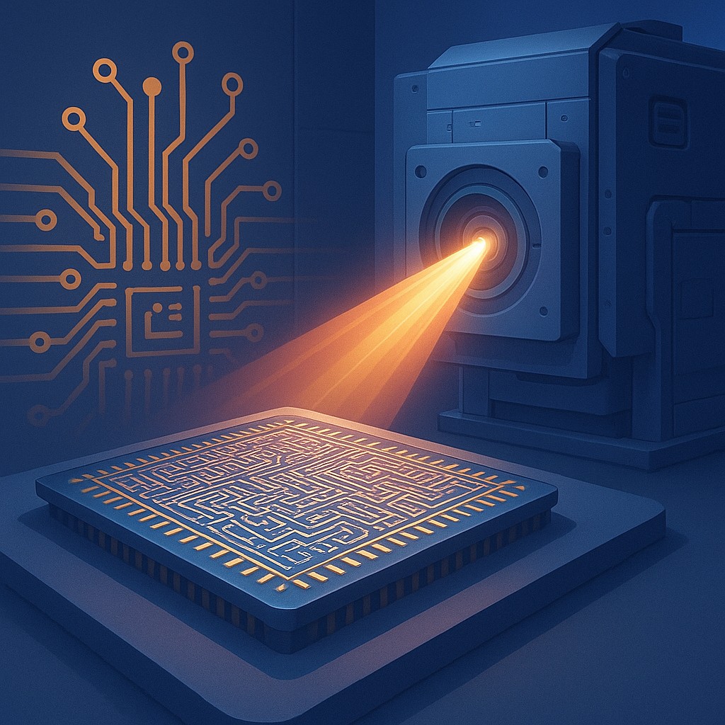
The tool currently taking center stage in this microscopic theater is called High-NA EUV lithography. It is a machine the size of a double-decker bus, costs hundreds of millions of dollars, and is arguably the most complex piece of equipment ever designed. To understand why it matters, we have to look past the shiny glass of our smartphones and into the heart of the silicon chip. For decades, engineers followed Moore’s Law, the observation that the number of transistors on a chip doubles roughly every two years. But light itself has become a bottleneck. We are now using light with such a short wavelength that it behaves less like a gentle ray and more like a high-energy structural beam. This has forced us to completely rethink how we manipulate the world at the atomic scale.
The Problem With Big Light and Tiny Spaces
To understand how lithography works, think of it as a high-tech game of shadow puppets. Scientists take a silicon wafer (a thin disc of silicon), coat it with a light-sensitive material called "photoresist," and then shine light through a mask containing the chip's design. Where the light hits the wafer, the material hardens or softens, allowing us to etch away the excess and leave behind the complex circuitry.
The problem is that standard light is "fat." If you try to draw a thin line with a thick marker, your lines blur together. For years, the industry used Deep Ultraviolet (DUV) light, which has a wavelength of 193 nanometers. When you are trying to print features that are only 5 or 10 nanometers wide, using 193-nanometer light is like trying to perform heart surgery with a chainsaw.
This led to the development of Extreme Ultraviolet (EUV) light, which has a wavelength of just 13.5 nanometers. This was a massive leap, but as we push toward the next generation of super-dense chips, even standard EUV isn't sharp enough. This is where the "NA" in High-NA EUV comes in. NA stands for Numerical Aperture, which describes a lens's ability to collect and focus light. Think of it like a camera lens: a wider aperture lets in more light and allows for a sharper focus on a specific point. By increasing the Numerical Aperture from 0.33 to 0.55, engineers can focus the EUV beam with incredible precision, allowing them to cram even more transistors into the same tiny sliver of silicon.
Bouncing Off Perfection in a Total Void
The journey of an EUV light particle, or photon, is perhaps the most difficult commute in the universe. Because EUV light has such a short wavelength, it is absorbed by almost everything, including the air we breathe. If you tried to run an EUV machine in a normal room, the oxygen and nitrogen molecules would soak up the light like a sponge, leaving nothing to hit the silicon wafer.
Consequently, the entire interior of these machines must be a vacuum more pristine than outer space. There is no air, no dust, and no room for error. Every single component must be perfectly clean, as even a single speck of dust can act like a giant boulder, blocking the light and ruining an entire batch of chips.
Furthermore, EUV light cannot be focused with traditional glass lenses because the glass would simply absorb the light. Instead, the machine uses a series of the flattest mirrors ever created. These mirrors are made of dozens of alternating layers of silicon and molybdenum, engineered to reflect as much EUV light as possible. How flat are they? If one of these mirrors were the size of the United States, the largest "mountain" on its surface would be less than a millimeter tall. These mirrors move the light through the vacuum with surgical accuracy, bouncing it toward the wafer to print patterns smaller than a biological virus. This extreme environment is why these machines are so expensive; you aren't just buying a printer, you are buying a controlled slice of the void.
Comparing the Generations of Lithography
To see how much of a leap we are truly making, it helps to compare the evolutionary steps of this technology. Each jump in lithography requires a massive overhaul of chemistry, physics, and mechanical engineering. While the goal is always to make things smaller, the methods change drastically once we hit the wall of what physics allows.
| Feature |
Deep UV (DUV) |
Standard EUV |
High-NA EUV |
| Light Wavelength |
193 nm |
13.5 nm |
13.5 nm |
| Numerical Aperture |
1.35 (using water) |
0.33 |
0.55 |
| Minimum Feature Size |
~40 nm (single exposure) |
~13 nm |
~8 nm |
| Environment |
Air or Pure Water |
High Vacuum |
High Vacuum |
| Optical Element |
Glass Lenses |
Special Mirrors |
Giant Specialized Mirrors |
| Machine Cost |
~$50 - $80 Million |
~$150 - $200 Million |
~$350+ Million |
The shift from 0.33 NA to 0.55 NA might sound like a small tweak, but it requires a total redesign of the internal parts. In High-NA machines, the mirrors are significantly larger and must be held so steadily that they don't vibrate even a fraction of an atom's width during the process. To fit these larger mirrors without making the machine the size of a stadium, the system uses "anamorphic" optics, which shrink the image differently in one direction than the other. This complexity is the price we pay to keep shrinking our digital world.
Why We Care About Shorter Distances
You might wonder why we spend billions of dollars just to make things smaller. The answer lies in the physics of electricity and heat. Every time a transistor switches on or off to process data, it moves electrons. When electrons travel through a material, they hit resistance, which generates heat.
By shrinking the transistors and moving them closer together, the electrons have a shorter distance to travel. This reduces the energy required for each calculation and lowers the heat the chip gives off. This is why a modern smartphone has more computing power than a room-sized supercomputer from the 1990s while running on a tiny battery.
Moreover, the density provided by High-NA EUV is essential for the future of Artificial Intelligence. Large AI models require massive amounts of data processing. If we can fit more transistors onto a single chip, we can increase the "bandwidth" or the speed of the computer's brain. This allows AI to process information faster, which is crucial for everything from self-driving cars to medical tools. Without the ability to shrink these features down to the molecular level, we would hit a "power wall" where chips would get too hot to function or require more electricity than a small city just to run a standard server.
Myths of the Microscopic Frontier
Whenever a technology reaches this level of complexity, a few misconceptions tend to pop up. One common myth is that we are simply "shooting a laser" at the silicon. While a laser is involved in creating the EUV light, it is not what touches the chip. Instead, a high-powered laser blasts a tiny droplet of molten tin twice. The first hit flattens the tin, and the second hit vaporizes it into a plasma that emits the 13.5 nm light. It is a violent process that happens 50,000 times per second. We are essentially catching the "glow" from microscopic explosions and using that glow to draw our circuits.
Another misconception is that smaller always means better in a simple way. In reality, as we get smaller, we encounter "stochastic effects," which is just a way of saying that physics starts to get weird and unpredictable. At 2 nanometers, the light might not hit the surface evenly, leading to "photon shot noise," which causes errors in the pattern. This is why the move to High-NA isn't just about a bigger lens; it’s about better chemistry and smarter sensors to ensure that every single particle of light lands exactly where it belongs. We are no longer just building machines; we are negotiating with the laws of probability.
The Future of the Atomic Canvas
As we look ahead, High-NA EUV is more than just a tool; it is a bridge. It connects the silicon era we have known for fifty years to a future of quantum or biological computing. By mastering the ability to control matter at the molecular level, we are essentially learning how to write the software of the physical world.
The engineers and scientists working in these cleanrooms are the modern equivalent of cathedral builders, working on structures of immense complexity that will define our civilization for generations. Every time you send a text or stream a video, you are using the results of a process that involves exploding tin, perfect mirrors, and a vacuum purer than the space between stars. We are living in an age where the impossible has become the industry standard. As our tools get smaller, our potential only grows.