For decades, the tech world followed a simple, comforting rule known as Moore’s Law. It predicted that the number of transistors on a microchip would double roughly every two years. Like a steady metronome, this rhythm made our computers faster and our smartphones sleeker. Engineers managed this by shrinking every component, carving increasingly tiny pathways into silicon. Eventually, chip features became smaller than a virus, approaching the width of a single atom. Recently, however, that metronome has started to skip beats. We have hit the physical limit where electricity leaks through walls too thin to hold it, and the heat from these dense "silicon cities" threatens to melt the very circuits they power.
Because we can no longer shrink the "bricks" of our digital world without them crumbling, we have to rethink the entire blueprint for building computers. The industry is pivoting from a flat, sprawling suburban design to a high-rise urban strategy. Instead of trying to cram more features onto one massive slice of silicon, engineers are breaking processors into specialized pieces and stacking them vertically. This shift, called advanced packaging, is more than a manufacturing trick; it is a fundamental change in how we build our most complex machines. By looking upward, we can bypass the physical wall of miniaturization, turning the flat world of the microchip into a thriving, 3D metropolis.
The End of the Single Silicon Monolith
For a long time, the gold standard of chipmaking was the "monolith." Imagine a giant, single-story factory where every department is carved out of one continuous block of material. Traditional chips work this way. If there is a tiny flaw in one corner of that factory, the entire building is ruined and must be thrown away. As chips grew larger and more complex to handle AI and high-performance tasks, the "yield" - the percentage of perfect chips per batch - began to plummet. It became too expensive and difficult to make these massive slabs of silicon when a single speck of dust could ruin a thousand-dollar part.
To solve this, the industry is moving toward a strategy called "chiplets." Think of chiplets as high-tech Lego bricks. Instead of one giant chip, engineers create several smaller, specialized chips. Each one handles a specific task, such as processing data, storing memory, or managing communications. Because these pieces are smaller, they are much easier and cheaper to make with high precision. If one small chiplet is broken, you only toss that tiny piece, not the whole assembly. This modular approach lets designers mix and match technologies, using the most advanced, expensive processes only where necessary, while using older, reliable methods for simpler parts.
This transition marks the end of "one size fits all" silicon. By breaking the monolith, companies can innovate faster. They can update a processor’s memory without redesigning its entire "brain." This is a more sustainable and flexible way to keep pushing the boundaries of what computers can do. However, this modularity creates a new challenge: how do you get these separate pieces to talk to each other as fast as if they were still part of the same block? The answer lies in the invisible glue and the vertical elevators of advanced packaging.
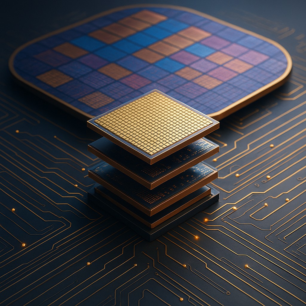
Building the Silicon Skyscraper with 3D Stacking
If chiplets are the rooms of our digital building, advanced packaging is the architecture that connects them. In a traditional setup, chips sat side-by-side on a printed circuit board, connected by long copper wires. These wires act like winding country roads. Data traveling along them takes time and uses a lot of energy. In high-speed computing, even a few millimeters of travel can feel like an eternity, creating a bottleneck that slows the system down. Advanced packaging eliminates these "commutes" by stacking the chips directly on top of one another.
This vertical stacking relies on technologies like Through-Silicon Vias (TSVs). Imagine these as microscopic elevator shafts that run straight through the floor and ceiling of each chiplet. Instead of traveling centimeters across a board, data only moves micrometers vertically to reach the next part. Because the distance is shorter, signals move faster and use much less power. When you stack memory directly on top of a processor, the "brain" can access its "memories" almost instantly, providing the speed needed for real-time AI and complex simulations.
There are different versions of this 3D architecture. In "2.5D" setups, chiplets sit on a specialized middle layer called an interposer, which acts as a high-speed data highway. In true 3D stacking, the chips are sometimes bonded directly, atom-to-atom. This creates a unified block of computing power that acts like a single chip but has the specialized strengths of many. It is the difference between a sprawling warehouse and a vertical data center, and it is the main reason performance keeps improving even though transistors have stopped shrinking.
Comparing Traditional and Advanced Packaging Architectures
To visualize how the industry is changing, it helps to look at the differences between the old way and the new, vertical frontier. The table below compares these two approaches.
| Feature |
Traditional Packaging |
Advanced Packaging (3D/Chiplets) |
| Physical Layout |
Horizontal / Side-by-Side |
Vertical / Stacked |
| Connectors |
Long copper wires and solder balls |
Microscopic TSVs and Hybrid Bonding |
| Manufacturing |
Monolithic (One large chip) |
Heterogeneous (Mix of small chiplets) |
| Connection Density |
Low (Sparse connections) |
Extremely High (Dense elevator arrays) |
| Energy Efficiency |
High power loss over long distances |
Low power loss due to short paths |
| Flexibility |
Rigid; any change requires a full redesign |
Modular; chiplets can be swapped |
| Data Delay |
Higher (Data takes longer to travel) |
Ultra-low (Near-instant communication) |
The Thermal Hurdle and the Cooling Revolution
While stacking chips like pancakes sounds perfect, it creates one massive problem: heat. In a traditional flat chip, every part has a direct path to the surface, where a fan or a metal heat sink can pull the warmth away. But when you stack several high-performance chips, the ones in the middle are trapped. They are surrounded by other heat-generating chips with no easy way to vent. If you run a 3D-stacked chip at full speed without a plan, it can quickly get hot enough to fail or damage the delicate bonds holding the stack together.
To solve this, engineers are getting creative with "thermal management." Some designs include "dummy" chiplets or specialized layers meant only to pull heat away from the center of the stack. Others are testing microfluidic cooling, where tiny channels are etched into the silicon so a cooling liquid can flow through the heart of the processor. This essentially gives the chip its own circulatory system to keep temperatures stable. This is a very active area of research, as the ability to stack chips is currently limited by our ability to keep the bottom chips from cooking the top ones.
Beyond liquid cooling, designers use "dark silicon" strategies. This plan involves intentionally powering down or slowing parts of the chip when they aren't needed to stay within a safe temperature range. Software and hardware must now work together to move tasks around the 3D structure, ensuring no single "neighborhood" in the silicon skyscraper gets too hot. Solving this thermal bottleneck is the key to the next decade of computing power, driving a new wave of research in materials science and mechanical engineering.
A New Map for Global Technology Production
The shift toward advanced packaging is both a scientific and a geopolitical evolution. For decades, the most advanced part of making a chip was the "front end" - printing transistors onto silicon. The "back end" - cutting and packaging the chips - was seen as a low-tech job and was often outsourced. But now that the package itself determines performance, packaging has become a high-stakes, high-tech industry.
We are seeing a massive effort to bring this work back to home soil. Countries realize that having the best transistor-printing machines isn't enough if they don't have the facilities to stack them into 3D structures. Governments are investing billions to build advanced packaging plants, recognizing them as the "crown jewel" of manufacturing. The ability to assemble chiplets from different sources into one high-performance package is the new frontier for national security. It ensures supply chains are strong and that sensitive technologies are built using the most secure, advanced methods.
As we move forward, the definition of a "chipmaker" is changing. Companies that once only focused on design are now becoming masters of architecture. The factories of the future will look less like assembly lines and more like high-tech labs. The move from flat to 3D is a change in how we think about human ingenuity. We are no longer just fighting against the size of the atom; we are learning to build upward. We are creating a vertical future where the only limit is our ability to imagine new ways to connect the pieces.
You are witnessing a historic pivot in technology, a moment where "smaller" is being replaced by "smarter." By moving from monolithic blocks to 3D-stacked chiplets, we are building the framework for the next generation of AI, medical breakthroughs, and massive simulations. This isn't just about faster computers; it is about human problem-solving. When we hit a wall, we don't stop; we build over, around, and through it. The silicon skyscraper is rising, proving that our potential for innovation is as infinite as the vertical space we are just beginning to explore.