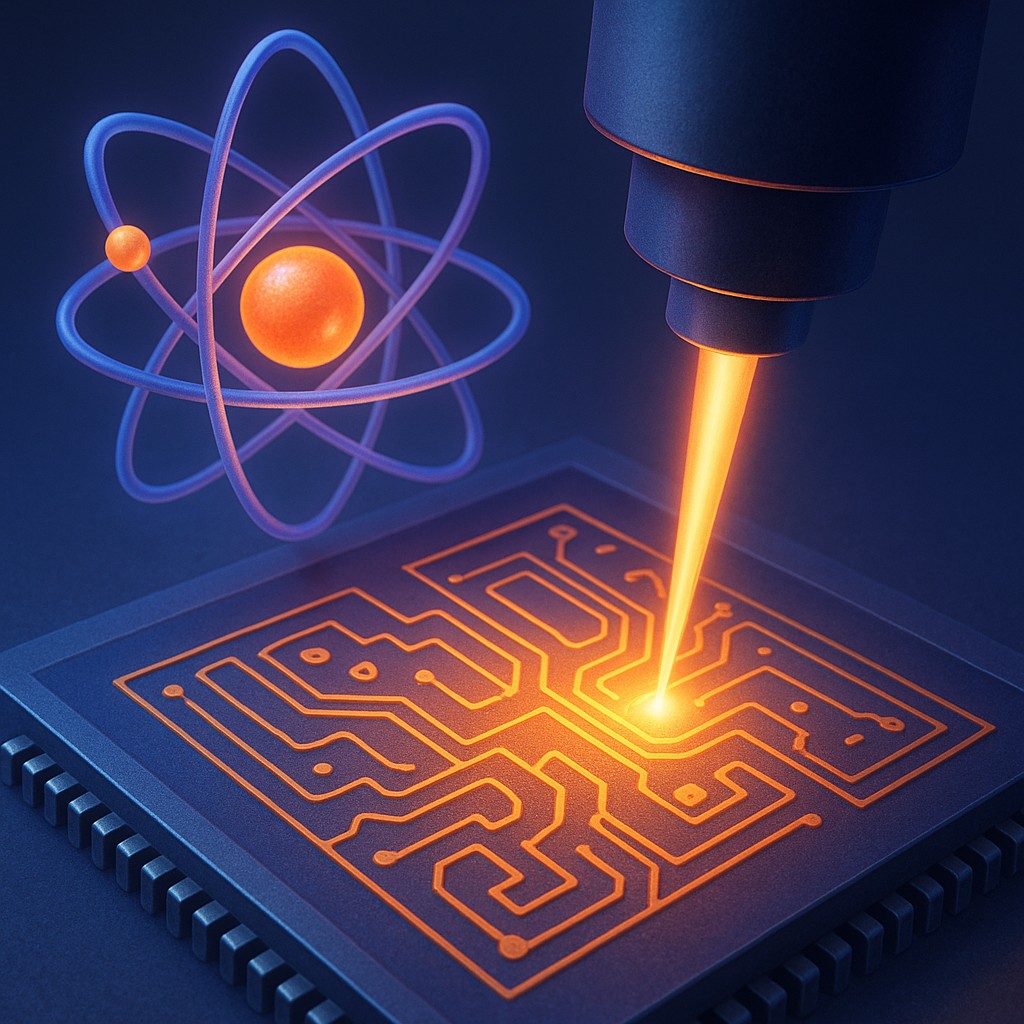
Imagine trying to write the entire Encyclopedia Britannica on the head of a pin using a fat permanent marker. No matter how steady your hand is, the tip of the pen is simply too wide to create legible letters at that scale. This is the fundamental crisis semiconductor engineers have faced for the last decade. As we demand smartphones that process billions of tasks per second and AI models that think instantly, the "pens" used to draw the internal circuitry of computer chips have become too thick. We have reached a point where the light used in manufacturing is literally too large to draw the features we need.
To solve this, the technology industry has entered a realm of physics that sounds more like science fiction than factory work. Engineers are now using "High-NA Extreme Ultraviolet" (EUV) lithography. This process involves vaporizing molten metal with high-powered lasers to create a light source so delicate that oxygen can absorb it. This light has a wavelength so small that it is measured against the width of individual atoms. By mastering this invisible, temperamental light, manufacturers can pack tens of billions of transistors onto a slice of silicon the size of a fingernail. This allows technological progress to continue even as we hit the hard limits of the physical world.
The Wavelength Wall and the Need for Finer Pens
In traditional chip making, we use a process called photolithography. Think of this as a high-tech stencil. We take a flat wafer of silicon, coat it with a light-sensitive chemical called a photoresist, and then shine light through a mask containing the circuit design. Where the light hits the chemical, it hardens or dissolves, leaving behind the blueprint of a microprocessor. For years, the industry used Deep Ultraviolet (DUV) light, which has a wavelength of 193 nanometers. This worked perfectly until the features we wanted to draw became smaller than the light itself. When your brush is wider than the line you are trying to paint, the edges become blurry and the circuit fails.
To bypass this physical limit, engineers spent years using "multi-patterning." This is essentially like drawing the same line four times with different stencils to make it look sharper. It was expensive, slow, and prone to errors. The shift to Extreme Ultraviolet (EUV) light changed everything by shrinking the wavelength from 193 nanometers down to a mere 13.5 nanometers. This is roughly the width of a few dozen atoms. Suddenly, the "marker" was fine enough to draw incredibly complex designs in a single pass. However, moving to such a small wavelength meant every rule of optics had to be rewritten, because this light behaves differently than anything ever used in a factory.
Catching Lightning by Exploding Tin Drops
Generating EUV light is perhaps the most violent and complex part of the entire manufacturing process. Because 13.5-nanometer light does not occur naturally on Earth in a usable way, we have to manufacture it from scratch inside a vacuum. The process begins with a tiny droplet of molten tin, about 30 microns wide, falling through a pressurized chamber. As it drops, a high-power laser strikes the tin twice. The first "pre-pulse" hit flattens the droplet into a pancake shape, and the second, much more powerful hit vaporizes it into a scorching plasma.
This plasma is briefly hotter than the surface of the sun. As it cools, it emits the necessary EUV radiation. This sequence happens 50,000 times every second to create a steady beam of light. It is a feat of timing and precision that borders on the impossible. If the laser is off by a fraction of a microsecond, or if the tin droplet is slightly misshapen, the light disappears. Furthermore, this light is so fragile that air molecules will stop it in its tracks. The entire machine must be kept in a vacuum clearer than outer space just to allow the light to travel from the plasma source to the silicon wafer.
The World’s Smoothest Mirrors and the High-NA Breakthrough
Once we have our EUV light, we face another massive problem: glass lenses do not work. In a standard camera or a pair of glasses, light passes through glass to be focused. But EUV light carries so much energy that glass absorbs it rather than bending it. To move the light through the machine, engineers had to develop a system of mirrors instead. These are not bathroom mirrors; they are layered with special materials like molybdenum and silicon to reflect specific wavelengths. They are also arguably the flattest objects ever created. If one of these mirrors were the size of the United States, the tallest "mountain" on its surface would be less than a millimeter high.
The "High-NA" in the latest generation of these machines stands for High Numerical Aperture. In photography, a lens with a higher numerical aperture can gather more light and show finer details. In chip making, increasing the NA from 0.33 to 0.55 allows the machine to project even smaller images onto the chip. This sounds like a minor update, but it requires a total redesign of the machine’s optics. The mirrors must be larger and the angles more extreme, allowing for the printing of features that are 1.7 times smaller than what was possible just a few years ago. This leap allows the industry to move toward "2-nanometer" processes and beyond.
| Feature |
Deep UV (Older Tech) |
Standard EUV (Current) |
High-NA EUV (Cutting Edge) |
| Wavelength |
193 nm |
13.5 nm |
13.5 nm |
| Numerical Aperture |
~1.35 (using water) |
0.33 |
0.55 |
| Resolution Limit |
~40 nm (single print) |
~13 nm |
~8 nm |
| Atmosphere |
Normal Air/Water |
Deep Vacuum |
Deep Vacuum |
| Optics |
Standard Glass Lenses |
Reflective Mirrors |
Larger, Precision Mirrors |
The Efficiency Tradeoff and the Energy Hunger
Powering a High-NA EUV machine is a monumental task that highlights the hidden costs of the digital age. These machines are about the size of a double-decker bus and weigh over 160 tons. They are packed with hundreds of thousands of parts, but their energy consumption is the most striking detail. Because the process of turning tin into plasma is inefficient, and because even the world’s best mirrors absorb about 30 percent of the light that hits them, you have to pump in a massive amount of electricity to get a tiny bit of usable light.
To produce just a few hundred watts of EUV light, the system requires over one megawatt of electricity. That is enough to power a small town. This creates a fascinating contradiction: the chips produced by these machines are incredibly energy-efficient, using less power to run apps and keeping phones cool, but the factories that make them have a carbon footprint that is growing rapidly. Manufacturers are currently racing to find ways to make the laser systems more efficient, but for now, the price of "smaller and faster" is a staggering demand on the power grid.
Seeing the Invisible Architecture of the Future
Why do we go through all this trouble just to make a switch a few atoms smaller? The answer lies in how electricity moves. When a transistor is smaller, electrons have a shorter distance to travel, which means the "switch" can flip faster. More importantly, smaller transistors need less voltage to operate. In high-performance computing, heat is the ultimate enemy. If we can make transistors smaller, we can pack more of them together without the chip melting, leading to the massive leaps in AI processing and graphics we see today.
As move toward the middle of the decade, the first High-NA EUV machines are being installed in "fabs" (semiconductor factories) around the world. These facilities are the cathedrals of the modern age. They cost billions of dollars to build and require a level of cleanliness that makes a hospital operating room look like a dusty attic. We are no longer just building tools; we are manipulating matter at a scale where the classical laws of physics begin to blur. Every time you send a message or use a digital tool, you benefit from a process involving exploding metal, space-age vacuums, and mirrors so flat they defy imagination.
Looking at the scale of this engineering triumph changes how we see the devices in our pockets. We have successfully turned the chaotic energy of plasma and the strange properties of ultraviolet light into a precision tool for human thought. The journey from "blunt" light to High-NA EUV shows our refusal to accept physical limits. As long as there is a need for more data and faster answers, we will find ways to carve our will into the heart of the atom, proving that with enough ingenuity, even the invisible can be mastered for the future.